Astra Machina Micro SR100 Series Evaluation Platform Kit RevC
Introduction
The Synaptics Astra™ SR100 Series of AI MCUs is designed to deliver high-performance, AI-Native, multimodal compute to consumer, enterprise, and industrial Internet of Things (IoT) workloads. Based on Arm® Cortex®-M55 cores with Helium™ technology and Arm Ethos™-U55 neural network processors (NPU), the MCUs feature multiple tiers of operation—performance, efficiency, low-power (LP) sensing, and always-on (AON)—that algorithmically deliver intelligence at every power level, to enable a new class of context-aware IoT devices. The AI-Native SR100 Series supports a rich set of peripherals and accelerators, including dual MIPI camera interfaces, image processing with encode and pre-roll, motion and voice activity detection engines, and industry-standard security. These features make it well-suited for streaming vision and audio processing applications at the IoT device edge.
The SR100 Series is a high-performance, ultra-low power, and small footprint Audio and Vision AI processor family.
Scope
This user guide describes the hardware configuration and functional details for the Astra Machina Micro SR100 Series Rev C and later Evaluation Platform Kit, and supported daughter cards, along with the bring-up sequence.
Definition of Board Components
Astra Machina Micro SR100 Series: Combined system with Micro Development Kit and supported daughter cards.
Micro Evaluation Platform Kit: Processor subsystem module with key components including SR110, QSPI, PSRAM and various standard hardware interfaces, buttons, headers, and power-in.
Daughter card: Add-on boards for supporting various features such as connectivity, debug, images sensors and other flexible I/O options.
Astra Machina Micro Evaluation Platform Overview
This section covers system features, block diagrams, and board views of the Astra Machina Micro SR100 Series platform.
Figure 1. Dimensions: W x H = 59.55 mm x 51 mm
Features
The Astra Machina Micro SR100 Series Evaluation Platform Kit includes the following components:
Main components on Machina Micro:
Synaptics SR110 (122-FCCSP) Audio & Vision AI processor
Debug IC: Synaptics SR100 (84-WCCSP)
Storage: 128 Mbit QSPI NOR Flash
PSRAM: 64 Mbit HyperRAM™ x8, 200 MHz
PMIC: Buck-Boost DC/DC for SR110 VBAT
Highly sensitive ambient light sensor: TCS34303
3-axis accelerometer: MC3479
M.2 E-key 2230 receptacle: Supports SDIO, UART, and PCM for Wi-Fi/BT modules
2 × USB 2.0 Type-C™ ports: One for SR110 Audio & Vision processor, other for Debug IC. Both provide system power.
Push buttons for system reset, wake-up, and user control
Slide switches for bootstraps, mute control, and power enable
Daughter card interface options:
2 × MIPI CSI-2® 2-lane RX interfaces (1.5 Gb/s max bandwidth): CSI0 on Samtec™ connector (shared with DVP), CSI1 on 15-pin FPC connector
1 × MIPI CSI-2® TX interface (1.5 Gb/s max bandwidth) on 15-pin FPC connector
SWD JTAG
2 × 20-pin headers with GPIOs are for additional application
4-pin header for UART debugging
3-pin header for PIR
System power supply:
USB Type-C
2-pin, 2.0 mm pitch header for 1-cell Li-ion battery
3-pin header for system power source selection
SR110 System Block Diagram
Figure 2. SR110 system block diagram
Top View of Astra Machina Micro SR110
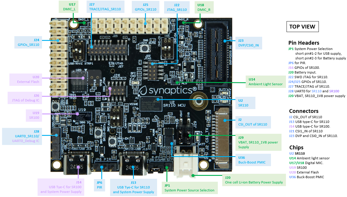
Figure 3. Headers, Connectors, Chips (Top view)

Figure 4. LEDs, Pushbuttons, Switches (Top view)
Bottom View of Astra Machina Micro SR110

Figure 5. Connectors, Chips (Bottom view)
Astra Machina Board Control/Status & System I/O
This section covers boot-up procedures, LED status indicators, buttons, connectors, and pin-strap settings.
Bootup Mode
The Astra Machina Micro SR110 supports two bootup modes. ROM mode, SR110 receives program code from external host over host interface (UART, I2C Slave, SPI Slave), and normal application mode, which boots directly from the onboard QSPI flash.
ROM mode: Set STRAP1 to High by closing switch of SW1-2,3. Then, power up the system and press the PMU_EN button, SW7 if SW1-1,4 is open position. Otherwise, pressing SW7 is not required.
Normal mode: Set STRAP1 to Low, then power up the system and press the PMU_EN button, SW7 if SW1-1,4 is open position. Otherwise, pressing SW7 is not required.
The strap settings are listed in Table 1.
Pad Name |
Strap Name |
Setting Value |
Resistor Stuffing + stuffed - removed |
Description Rpu = OnChip Pull-up Rpd = OnChip Pull-down |
|---|---|---|---|---|
I2S_DO |
STRAP0 |
— 0* 1 |
— -R5 +R5 |
Straps for PLL frequency (If TEST_N=1) 0: 200 MHz 1: 24 MHz |
SD0_CLK |
STRAP1 |
— 0* 1 |
— SW1, pin2 OFF SW1, pin2 ON |
Straps for booting up mode (If TEST_N=1) 0: boot from QSPI 1: boot from external host |
Indicates the default value.
LEDs
LED locations
Figure 6 shows the LED locations on Astra Machina Micro.

Figure 6. LED locations (Top View)
LED definitions
LED |
Color |
LED Functions |
|---|---|---|
D1 |
RED |
User definable Red LED. |
D2 |
Green |
User definable Green LED. |
D30 |
BLUE |
light up when main SR110_USB and whole system are both powered. |
D31 |
Green |
light up when Li-ion battery is plugged-in and whole system are both powered. |
D32 |
RED |
light up when Debug IC USB is powered. |
D33 |
Green |
Flash during QSPI (SPI_CS0) access. |
Hardware Manual Slide Switch Settings
Switch Block |
Pin # |
Function |
Description |
|---|---|---|---|
SW1 |
1 2 |
USB wake up main SR110 Main SR110 STRAP1 |
OFF: Disconnect USBPWR to PMU_EN (Default) ON: Enable USBPWR to PMU_EN OFF: Boot from QSPI (Default) ON: Boot from external Host |
SW2 |
1 2 |
Camera Mute Audio Mute |
OFF: De-mute Camera (Default) ON: Mute Camera OFF: De-mute Audio (Default) ON: Mute Audio |
SW5 |
1 2 |
DMIC Data DMIC Clock |
OFF: Cut-off DMIC data from MCU (Default) ON: Link up DMIC data with MCU OFF: Cut-off DMIC clock from MCU (Default) ON: Link up DMIC clock with MCU |
A white circui |
board |
ith green squares AI- |
enerated content may |
incorrect.|
Figure 8. Slide switch locations on Machina Micro board
Hardware Jumper Settings
This section outlines the board’s hardware jumper settings.
Ref Des |
Type |
Function |
Configuration |
Description |
|---|---|---|---|---|
JP1 |
3x1, pitch 2.54mm header |
System power source selection |
1-2 2-3 |
System power is from USB Connector. (Default) System power is from Battery. |
J29 |
2x2, pitch 2.54mm header |
Power source Jumpers |
1-2 3-4 |
Supply power to SR110 VBAT (Default) Supply Internal 1.8V LDO to source SR110 1V8 supply rail (Default) |
Figure 9 shows the Header locations on the board.
Figure 9. Jumper Locations (Top View)
SR110 Machina Micro Platform Connectors
This section shows the connector locations on the board.
Connector locations on the Top Side
Figure 10. Connector Locations (Top Side)
Connector Locations on the Bottom Side
Figure 11. Connector Locations (Bottom Side)
Connector Definitions – Astra Machina Micro Platform
Main Ref Des |
Connecting Boards/Devices (Ref Des if any) |
Function |
Remarks |
|---|---|---|---|
J2 |
CSI receiver module |
CSI output |
2 lane CSI output to FCC connector. |
J4 |
M.2 2230 D/C |
SDIO, PCM and UART |
1x1/2x2 WiFi/Bluetooth card via SDIO and UART/PCM. |
JP6 |
PIR module |
PIR |
For PIR input trigger. |
J13 |
USB type-C Host |
USB2.0 device, 5V power supply |
Main SR110 USB2.0 device mode and system 5V input. |
J14 |
USB type-C Host |
USB2.0 device, 5V power supply and Debug Port |
Debug IC USB2.0 device mode and system 5V input. |
J20 |
Li-ion Battery |
Battery power |
Pitch 2.0mm header for 1 cell Li-ion Battery. |
J21 |
Camera module |
CSI1_RX |
Raspberry-pi compatible 2-lanes CSI input. |
J22 |
Off board debugger connect |
SWD JTAG |
Connector for off board debugger such as JLink for SR110 |
J23 |
Camera modules |
CSI0_RX and DVP |
2-lanes CSI input and 8bit DVP input |
J24, J25 |
20 pin headers |
General-purpose I/O pins interface |
I2S, I2C, SPI, SDIO, UART, GPIOs, SPI, CIU, SWIRE |
J26 |
Off board debugger connect |
SWD JTAG |
Connector for off board debugger such as Jlink for Debug IC. |
J27 |
Off board Trace Module |
SR110 debug + ETM |
JTAG and Embedded Trace Macrocell (ETM) TRACECLK and TRACEDATA(n) signals. |
J28 |
UART |
UART0 |
Shared UART0 from main SR110 MCU and Debug IC. |
J29 |
Power Sources |
Power Source Jumpers |
Apply 3.3V to VBAT and use internal 1.8V LDO to supply 1.8V input rail of the SR110 |
Stuffing Options for SR110 Machina Micro Platform Power Measurement
There are 0-ohm serial resisters on power rails that can be replaced with power meter for power measurement.
Power Rail Name |
Description |
Stuffing Option |
Implementation |
|---|---|---|---|
VBAT |
3.3V power for SR110_VBAT. |
JP29 #1-2 |
Replace jumper with power meter |
1.8V Supply Rail |
Internal 1.8V LDO to supply 1.8V input rail of the SR110 |
JP29 #3-4 |
Replace jumper with power meter |
SR110_VDDIO1P8 |
1.8V power that SR110 VDDIO needs. |
R6 |
Replace R6 with power meter. |
VDD_CORE |
0.8V power that SR110 Core needs. |
R8 |
Replace R8 with power meter. |
V_DMIC |
1.8V power that DMICs need |
R1950 |
Replace R1950 with power meter. |
VDDA |
Analog power that SR110 needs. |
R9 |
Replace R9 with power meter. |
SYS_3V3_DVP |
3.3V power supply to Camera module on J23. |
R1904 |
Replace R1904 with power meter. |
SYS_1V8_CSI_OUT |
1.8V power supply to CSI transmitter on J2. |
R1907 |
Replace R1907 with power meter. |
SYS_3V3_CSI1 |
3.3V power supply to Camera module on J21. |
R1906 |
Replace R1906 with power meter. |
PWR_M2-KEYE_3V3 |
System power (4.8V~2.8V) supply to WiFi module on J4 |
R1852 |
Replace R1852 with power meter. |
SYS_1V8_JTAG |
1.8V power supply to JTAG debug. |
R1861 |
Replace R1861 with power meter. |
DBG_SYS_1V8 |
1.8V power that Debug IC sus-system needs. |
R177 |
Replace R177 with power meter. |
SYS_PWR_SRC |
Total power (4.8V~2.8V) that main SR110 system needs. |
JP1 #1-2 JP1 #2-3 |
If system power comes from USB, attach two probes of power meter to JP1#1 and #2. If system power comes from Battery, attach two probes of power meter to JP1#2 and #3. |
SR110_VDDH_USB |
1.8V power for SR110 USB |
R1858 |
Replace R1858 with power meter |
QSPI_1V8 |
1.8V power for QSPI |
R1947 |
Replace R1947 with power meter |
PWR_M2-KEYE_VIO |
1.8V VIO Power to M2 |
R1975 |
Replace R1975 with power meter. |
A white circuit |
oard with red an |
blue symbols AI |
generated conten |
may be incorrect.|
Figure 12. Probe points (Top side)

Figure 13. Probe points (Bottom side)
Daughter Cards
A set of daughter cards supplements (not included) the Astra Machina system with a range of extensible and configurable functionalities including Wi-Fi and Bluetooth connectivity, debug options and general purpose I/O. Details of currently supported daughter cards are described in this section.
Debug Board
Different kinds of debug interfaces are routed out for users to communicate with the SR110 system. The 20-pin SR110 debug + ETM header, J27 can be used to access the Embedded Trace Macrocell (ETM) TRACECLK and TRACEDATA(n) signals. The four TRACEDATA signals provide a high-speed data path for capturing instructions.
J22, 10-pin SWD JTAG header, allows connection to a 10-pin ARM debug connector for the debugging application SR110.
Users may communicate with SR110 over UART on a PC host by using a UART to USB cable commonly available. For a list of qualified parts, see the Astra Machina webpage.
UART on the Machina Micro board and the PC host USB are digitally isolated, with no direct conductive path, eliminating ground loop and back-drive issues when either is powered down.
USB device port is also available for PC host to communicate directly though type-C to type-A cable.
Figure 14 shows debug board connectivity facilitating UART and JTAG communications.
UART to USB adaptors/modules mentioned in the Knowledge base support only TTL 3.3V UART signals. UART signals of SR110 Machina Micro Platform are 1.8V CMOS. CP2102 and CH340G are not compatible with SR110 Machina Micro.
Figure 14. Debug board connectivity for UART and JTAG
Onboard Debug and Programming Interface via Debug IC, SR100 (SWD + UART)
The Astra Machina Micro platform incorporates a flexible and robust debug architecture that offers an onboard option to program and debug the SR110 SoC using Serial Wire Debug (SWD). This is achieved through the inclusion of a dedicated debug IC, specifically the SR100, which serves as a bridge between external PCs and the SR110. The SR100 acts as a USB to SWD bridge, with the PC connected over USB, and the SR110 connected via SWD. This emulates the behavior of widely used debug probes such as the SEGGER J-Link.
By leveraging this built-in debugging path, the system enables seamless access to the SR110’s core and peripheral registers for firmware development, bring-up, and system-level debugging—without the need for external debug hardware connections directly to the SoC.
In addition to acting as a USB to SWD bridge the debug SR100 also acts as a USB to UART bridge. The firmware on the SR100 uses the USB CDC class to emulate two com ports. After connecting a PC to the debug SR100 USB (J14), two com ports enumerate on the PC. The first com port is for UART0, and the second for UART1.
UART0 can be used to program the SR110 when STRAP1 is set to ROM mode. When STRAP1 is not in ROM mode UART0 can also be used to communicate with the Host API running on SR110, if the FW configures UART0 for the Host API communication interface. UART1 can be used to capture logs from the SR110.
Figure 15. DAP Block Diagram
Table 8. Serial Wire Debug (TCK/TMS) Signal Paths: Debug IC ↔ SR110
SWD |
Debug IC |
SR110 |
J22 Header |
|---|---|---|---|
TCK |
U19-H12 (GPIO[6]) |
U2-C17 |
J22-4 |
TMS |
U19-K12 (GPIO[7]) |
U2-B18 |
J22-2 |
RSTn |
U19-H6 (GPIO[27]) |
U2-J1 |
— |
M.2 Card
An M.2 E-Key socket J4 is provided for a variety of modules in the M.2 form factor. Typical applicable modules support Wi-Fi/BT devices with SDIO interfaces.
Available module:
Ampak AP12611_M2P with SYN43711 1x1 WiFi6E/BT5.3 1x1 over SDIO on M.2 adaptor (not included).
Figure 16. WiFi module plugged in M.2 slot
Camera Module
Two camera interfaces DVP and CSI0 (not included) are both routed out to J23, that allowed developer to switch their own camera module which has the matched pin sequence. Machina Micro Evaluation Platform can do person detection with the default attached camera module OV02C10, which is mounted on the platform through a small Samtec daughter card. Please take care about the connecter pin definition between module and daughter card, daughter card pin #24 should connect to module’s pin #12, instead of pin #1 to pin #1.
Figure 17. Camera daughter card with module OV02C10 on Machina Micro board
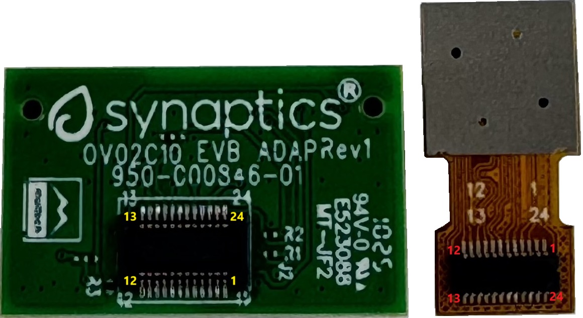
Figure 18. Connector between Camera daughter card and module OV02C10
General Purpose 20-pin Header
Two general-purpose 20-pin GPIO headers with a 0.1-inch (2.54 mm) pin pitch are located on the left and top edges of the Machina Micro board. All general-purpose I/O pins operate at 1.8V and can be configured in software to support a variety of alternate functions.
For detailed configuration options, refer to the SR100 Series Datasheet.

Figure 19. General Purpose J24, 20-Pin Header with Signal Mapping
Figure 20. General Purpose J25, 20-Pin Header with Signal Mapping
Pin Demuxing for Standard Interface Configuration
This section covers pin-demuxing configuration for the Machina Micro SR110 board.
Ball Name |
NetNames |
Reference Destination |
Function |
Pin Multiplexer Mode* |
Notes |
|---|---|---|---|---|---|
AUDIO_MUTE |
SR110_AUDIO_MUTE |
SW2-1,4 |
Audio Mute |
ALT 0 (GPIO); Any |
Mute |
CAMERA_MUTE |
SR110_CAMERA_MUTE |
SW2-2,3 |
Camera Mute |
ALT 0 (GPIO); Any |
|
CIU_D3 |
SR110_GPIO10.CIU_D3 |
J23-31 J25-2 |
DVP Connector, D3 20 Pin Header |
ALT 1 ALT 0 (GPIO); Any |
— — |
CIU_D6 |
SR110_GPIO13. CIU_D6.DM0_CLK_B |
J23-17 SW5-1,4 J25-17 U19-H8 |
DVP Connector, D6 Connect DMIC CLK 20 Pin Header Logger UART TX to Debug IC |
ALT 1 ALT 2 ALT 0 (GPIO); Any ALT 3 |
Cannot simultaneously operate DVP, DMIC, and UART1 Logger. Only one can run at a time |
CIU_D7 |
SR110_GPIO14.CIU_D7.DM0_DATA_B |
J23-15 SW5-2,3 JP25-18 U19-G9 |
DVP Connector, D7 Connect DMIC DATA 20 Pin Header Logger UART RX to Debug IC |
ALT 1 ALT 2 ALT 0 (GPIO); Any ALT 3 |
Cannot simultaneously operate DVP, DMIC, and UART1 Logger. Only one can run at a time |
CIU_VSYNC |
SR110_GPIO4.CIU_VSYNC_A |
J23-35 J25-5 J4-34 J23-40 |
DVP Connector, VSYNC 20 Pin Header M.2 UART_CTS (BT/BLE) DVP Connector, VSYNC |
ALT 1 ALT 0 (GPIO); Any ALT 3 ALT 1 |
Cannot simultaneously operate DVP and M.2 UART (BT/BLE) Not populated by default |
CLK32K_IN |
SR110_GPIO40. CLK32KIN |
J24-17 |
20 Pin Header |
ALT 0 (GPIO); Any |
— |
CLKOUT0 |
SR110_GPIO41 .CLKOUT0 |
J23-7 J24-15 |
DVP Connector, Clock 20 Pin Header |
ALT 1 ALT 0 (GPIO); Any |
— — |
CSI_OUT_CN |
SR110_CSI_OUT_CN |
J2-8 |
— |
— |
CSI_OUT |
CSI_OUT_CP |
SR110_CSI_OUT_CP |
J2-9 |
— |
— |
|
CSI_OUT_D0N |
SR110_CSI_OUT_D0N |
J2-2 |
— |
— |
|
CSI_OUT_D0P |
SR110_CSI_OUT_D0P |
J2-3 |
— |
— |
|
CSI_OUT_D1N |
SR110_CSI_OUT_D1N |
J2-5 |
— |
— |
|
CSI_OUT_D1P |
SR110_CSI_OUT_D1P |
J2-6 |
— |
— |
|
CSI0_IN_CN |
SR110_CSI0_IN_CN |
J23-22 |
— |
— |
CSI0_IN |
CSI0_IN_CP |
SR110_CSI0_IN_CP |
J23-20 |
— |
— |
|
CSI0_IN_D0N |
SR110_CSI0_IN_D0N |
J23-16 |
— |
— |
|
CSI0_IN_D0P |
SR110_CSI0_IN_D0P |
J23-14 |
— |
— |
|
CSI0_IN_D1N |
SR110_CSI0_IN_D1N |
J23-28 |
— |
— |
|
CSI0_IN_D1P |
SR110_CSI0_IN_D1P |
J23-26 |
— |
— |
|
CSI1_IN_CN |
SR110_CSI1_IN_CN |
J21-8 |
— |
— |
CSI1_IN |
CSI1_IN_CP |
SR110_CSI1_IN_CP |
J21-9 |
— |
— |
|
CSI1_IN_D0N |
SR110_CSI1_IN_D0N |
J21-2 |
— |
— |
|
CSI1_IN_D0P |
SR110_CSI1_IN_D0P |
J21-3 |
— |
— |
|
CSI1_IN_D1N |
SR110_CSI1_IN_D1N |
J21-5 |
— |
— |
|
CSI1_IN_D1P |
SR110_CSI1_IN_D1P |
J21-6 |
— |
— |
|
GPIO5 |
SR110_JTAG_TRSTN_A .CIU_HSYNC.GPIO5 |
J25-5 J23-37 J4-36 J22-10 |
20 Pin Header DVP Connector, HSYNC M.2 UART_RTS (BT/BLE) JTAG TRST |
ALT 2 ALT 1 ALT 3 ATL 0 |
Cannot simultaneously operate DVP and M.2 UART (BT/BLE) Cannot run JTAG with DVP or M.2UART |
GPIO6 |
SR110_GPIO6.CIU_BCLK.SPI_SLV_CLK_B |
J25-7 J23-38 J23-14 |
20 Pin Header DVP Connector, BCLK OV2C_D0p/SCLK |
ALT 0 (GPIO); Any ALT 1 ALT2 |
— — Not populated by default |
GPIO7 |
SR110_GPI O7.CIU_D0.SPI_SLV_MOSI_B |
J25-10 J23-39 J23-16 |
20 Pin Header DVP Connector, D0 OV2C_D0n/SDAT |
ALT 0 (GPIO); Any ALT 1 ALT 2 |
— — Not populated by default |
GPIO8 |
SR110_JTAG_TDI_A.CIU_D1.GPIO8.SPI_SLV_CS_B |
J23-40 J25-8 J22-10 |
DVP Connector, D1 20 Pin Header JTAG_TDI |
ALT 1 ALT 2 ALT 0 (GPIO); Any |
DVP cannot run while JTAG is active |
GPIO9 |
SR110_JTAG_TDO_A.CIU_D2.GPIO9.SPI_SLV_MISO_B |
J23-33 J22-6 J25-9 |
DVP Connector, D2 JTAG_TDO 20 Pin Header |
ALT 1 ALT 0 ALT 2 (GPIO); Any |
DVP cannot run while JTAG is active |
I2C_SLV_SCLI2C_PMU_SCL I3C_SLV_SCL |
SR110_GPIO45.I2C_PMU_SCL.UART0_TX_C |
J2-14 J4-32 J24-13 |
I2C Slave over RPI connector M.2 UART RX (BT/BLE) 20 Pin Header |
ALT 1 ALT 2 ALT 0 (GPIO); Any |
M.2 UART and RPI Connector I2C Slave cannot operate simultaneously |
I2C_SLV_SDAI2C_PMU_SCL I3C_SLV_SCL |
SR110_GPIO44.I2C_PMU_SDA.UART0_RX_C |
J2-15 J4-22 J24-14 |
I2C Slave over RPI connector M.2 UART RX (BT/BLE) 20 Pin Header |
ALT 1 ALT 2 ALT 0 (GPIO); Any |
M.2 UART and RPI Connector I2C Slave cannot operate simultaneously |
I2S_BCLK |
SR110_GPIO17. I2S_BCLK |
J27-20 J4-8 J24-3 |
Trace Data I2S to M.2 20 Pin Header |
ALT 2 ALT 1 ALT 0 (GPIO); Any |
I2S and Trace cannot operate simultaneously |
I2S_DI |
SR110_GPIO20.I2S_DI |
J4-14 J27-14 J24-24 |
I2S to M.2 Trace Data 20 Pin Header |
ALT 1 ALT 2 ALT 0 (GPIO); Any |
I2S and Trace cannot operate simultaneously |
I2S_D0 |
SR110_GPIO19.I2S_DO |
J4-14 J27-16 J24-5 |
I2S to M.2 Trace Data 20 Pin Header |
ALT 1 ALT 2 ALT 0 (GPIO); Any |
I2S and Trace cannot operate simultaneously |
I2S_FSYNC |
SR110_GPIO18.I2S_FSYNC |
J4-10 J27-18 J24-4 |
I2S to M.2 Trace Data 20 Pin Header |
ALT 1 ALT 2 ALT 0 (GPIO); Any |
I2S and Trace cannot operate simultaneously |
I2C0_MS_SCL |
SR110_GPIO15.I2C0_MS_SCL |
U7-3 J23-13 U16-19 U14-3 U31-1 U26.2 J25-3 SW5-1,4 |
Level Translator control of camera c onnected via RPI connector DVP connector, I2C camera control Port Expander ALS IMU RTC 20 Pin Header Connect DMIC CLK |
ALT 1 ALT 1 ALT 1 ALT 1 ALT 1 ALT 1 ALT 0 (GPIO); Any ALT3 |
— — — Not populated by default OV2C_D0p/SCLK — — — |
I2C0_MS_SDA |
SR110_GPIO16.I2C0_MS_SDA |
U7-4 J23-11 U16-20 U14-2 U31-4 U26.3 J25-4 SW5-2,3 |
Level Translator control of camera c onnected via RPI connector DVP connector, I2C camera control Port Expander ALS IMU RTC 20 Pin Header Connect DMIC DATA |
ALT 1 ALT 1 ALT 1 ALT 1 ALT 1 ALT 1 ALT 0 (GPIO); Any ALT3 |
— — — Not populated by default Not populated by default — — — |
JTAG_TCK |
SR110_GPIO31. JTAG_TCK |
J22-4 U19-H12 |
Debug Header SWD to Debug IC |
ALT 0 (GPIO); Any ALT 0 (GPIO); Any |
— — |
JTAG_TMS |
SR110_GPIO32. JTAG_TMS |
J22-2 U19-K12 |
Debug Header SWD to Debug IC |
ALT 0 (GPIO); Any ALT 0 (GPIO); Any |
— — |
PMU_EN |
SR110_PMU_EN |
SW1-1,4 |
If on PMU_EN will go high when USB is c onnected |
||
RESET_N |
SR110_RSTn |
U16-24 J22-7 U19-H6 |
Port Expander Debug Header Debug IC |
ALT 0 (GPIO); Any ALT 0 (GPIO); Any ALT 0 (GPIO); Any |
Not populated by default |
SD0_CLK |
SR110_GPIO26 .SD0_CLK |
SW1-2,3 J27-12 J24-8 |
Strap 1 Trace Data 20 Pin Header |
STRAP 1 ALT 3 ALT 0 (GPIO); Any |
Change programming mode — — |
SD0_CMD |
SR110_GPIO25 .SD0_CMD |
J24-7 J4-54 |
20 Pin Header M2- KEYE_W_DISABLE2n |
ALT 0 (GPIO); Any ALT 0 (GPIO); Any |
— — |
SD0_D0 |
SR110_GPIO27.SD0_D0 |
J24-9 |
20 Pin Header |
ALT 0 (GPIO); Any |
— |
SD0_D1 |
SR110_GPIO28.SD0_D1 |
J24-10 |
20 Pin Header |
ALT 0 (GPIO); Any |
— |
SD0_D2 |
SR110_GPIO29.SD0_D2 .DM1_CLK |
J24-11 |
20 Pin Header |
ALT 0 (GPIO); Any |
— |
SD0_D3 |
SR110_GPIO30 .SD0_D3. DM1_DATA |
J24-12 |
20 Pin Header |
ALT 0 (GPIO); Any |
— |
SD1_CLK |
R110_GPIO35 .SD1_CLK |
J4-9 |
M.2 SDIO |
ALT 1 |
— |
SD1_CMD |
SR110_GPIO34 .SD1_CMD |
J4-11 |
M.2 SDIO |
ALT 1 |
— |
SD1_D0 |
SR110_GPIO36.SD1_D0 |
J4-13 |
M.2 SDIO |
ALT 1 |
— |
SD1_D1 |
SR110_GPIO36.SD1_D1 |
J4-15 |
M.2 SDIO |
ALT 1 |
— |
SD1_D2 |
SR110_GPIO36.SD1_D2 |
J4-17 |
M.2 SDIO |
ALT 1 |
— |
SD1_D3 |
SR110_GPIO36.SD1_D3 |
J4-19 |
M.2 SDIO |
ALT 1 |
— |
SPI_MSTR_CLK |
SR110_GPIO22.SPI_MSTR_CL K.CIU_D5 |
J23-19 J25-11 |
DVP Connector, D5 20 Pin Header |
ALT 3 ALT 0 (GPIO); Any |
— — |
SPI_MSTR_CS |
SR110_GPIO21.SPI_MSTR_C S.CIU_D4 |
J2512 J23-23 |
DVP Connector, D4 20 Pin Header |
ALT 3 ALT 0 (GPIO); Any |
— — |
SPI_MSTR_MISO |
SR110_GPIO24.SPI_MSTR_M ISO.I2C1_MS_SDA. UART1_RX |
U14-2 (TCS34303) U31-4 (MC3479) J23-11 J25-13 |
ALS Sensor I2C IMU I2C DVP connector, I2C camera control 20 Pin Header |
ALT 3 ALT 3 ALT 3 ALT 0 (GPIO); Any |
— — Not populated by default — |
SPI_MSTR_MOSI |
SR110_GPIO23.SPI_MSTR_M OSI.I2C1_MS_SCL. UART1_TX |
U14-3 (TCS34303) U31-1 (MC3479) J25-14 |
ALS Sensor I2C IMU I2C 20 Pin Header |
ALT 3 ALT 3 ALT 0 (GPIO); Any |
— — — |
SPI_SLV_CLK |
SR110_AON_GPO1 |
SYS_PWR_MOS_EN (R1865) J24-16 |
System Power Enable 20 Pin Header |
ALT 5 ALT 0 (GPIO); Any |
— — |
SPI_SLV_CS |
SR110_GPIO3. AON_GPI1 |
U16-22(PI4IOE5V6416ZDEX) |
Port Expander Int |
ALT 0 (GPIO); Any |
— |
SPI_SLV_MISO |
SR110_GPIO0. UART0_TX_A.TESTn |
J28-2 U19-C9 |
UART Header Debug IC |
ALT 1 ALT 1 |
ROM Programming UART connect to Debug IC |
SPI_SLV_MOSI |
SR110_GPIO1.UART0_RX_A |
J28-3 R12 U19-B10 |
UART Header 4.7k Pull-Up to 1.8V Debug IC |
ALT 1 ALT 1 ALT 1 |
ROM Programming — UART connect to Debug IC |
SWIRE_CLK |
SR110_GPIO42.SWIRE_CLK |
J23-10 J25-15 U7-3 (PCA9306JKZ) U31-1 (MC3479) U14-3 (TCS34303) U16-19 (PI4IOE5V6416ZDEX) J23-13 |
DVP Connector 20 Pin Header I2C1_MS_SDL_B I2C1_MS_SDL_B I2C1_MS_SDL_B I2C1_MS_SDL_B DVP Connector |
ALT 3 ALT 0 (GPIO); Any ALT 3 ALT 3 ALT 3 ALT 3 ALT 3 |
— — — — — — — |
SWIRE_DATA |
SR110_GPIO43.SWIRE_DATA |
J4-54 J25-16 U7-4 (PCA9306JKZ) U31-4 (MC3479) U14-2 (TCS34303) U16-20 (PI4IOE5V6416ZDEX) J23-11 |
DVP Connector 20 Pin Header I2C1_MS_SDA_B I2C1_MS_SDA_B I2C1_MS_SDA_B I2C1_MS_SDA_B DVP Connector |
ALT 3 ALT 0 (GPIO); Any ALT 3 ALT 3 ALT 3 ALT 3 ALT 3 |
— — — — — — — |
USB_HS_DN |
SR110_USB_HS_DN |
J13 (USB Conn) |
— |
— |
— |
USB_HS_DP |
SR110_USB_HS_DP |
J13 (USB Conn) |
— |
— |
— |
VBAT |
SR110_VBAT_0 |
JP29-1 SW7 (Push Button: PMU EN) |
— — |
— — |
— — |
VDDH_USB |
SR110_VDDH_USB |
U28-1 SW1-1,2 ( PMU_EN) |
— — |
— — |
— — |
XSPI_CLK |
SR110_xSPI_CLK |
U4- B2(W956D8MBYA5I) U5-6 (GD25LQ128EWIGR) |
— — |
— — |
Not stuff by default — |
XSPI_CLKN |
SR110_x SPI_CLKn |
U4- B1(W956D8MBYA5I) |
— |
— |
Not populated by default |
XSPI_CS0N |
SR110_x SPI_CS0n |
U5-1 (GD25LQ128EWIGR) |
— |
— |
— |
XSPI_CS1N |
SR110_x SPI_CS1n |
U4(W956D8MBYA5I) |
— |
— |
Not populated by default |
XSPI_DATA0 |
SR110_xSPI_D0 |
U5-5 (GD25LQ128EWIGR) U4-D3 (W956D8MBYA5I) |
— — |
— — |
— Not populated by default |
XSPI_DATA1 |
SR110_xSPI_D1 |
U5-2 (GD25LQ128EWIGR) U4-D2 (W956D8MBYA5I) |
— — |
— — |
— Not populated by default |
XSPI_DATA2 |
SR110_xSPI_D2 |
U5-3 (GD25LQ128EWIGR) U4-C4 (W956D8MBYA5I) |
— — |
— — |
— Not populated by default |
XSPI_DATA3 |
SR110_xSPI_D3 |
U5-7 (GD25LQ128EWIGR) U4-D4 (W956D8MBYA5I) |
— — |
— — |
— Not populated by default |
XSPI_DATA4 |
SR110_xSPI_D4 |
U4(W956D8MBYA5I) |
— |
— |
External xSPI, HyperRAM Rev B: Available. Rev C: DNS (Desing not Stuff) |
XSPI_DATA5 |
SR110_xSPI_D |
— |
— |
||
XSPI_DATA6 |
SR110_xSPI_D6 |
— |
— |
||
XSPI_DATA7 |
SR110_xSPI_D7 |
— |
— |
||
XSPI_DQS |
SR110_xSPI_DQS |
— |
— |
GPIO Expanders Over I2C
Due to the considerable number of functionalities covered by Machina Micro SR110 platform, most of the SR110 digital pins that have GPIO/GPO pin-demux options are used for other functions. As such, GPIO expanders are used extensively to supplement system control purposes.
Expander GPIO/GPO |
I2C# |
Voltage |
Direction |
Function |
GPIO S ignaling |
|---|---|---|---|---|---|
GPIO0_0 |
I2C0 (0x20) |
1.8V |
OUT |
User definable Green LED |
0: OFF 1: ON |
GPIO0_1 |
I2C0 (0x20) |
1.8V |
OUT |
User definable Red LED |
0: OFF 1: ON |
GPIO0_2 |
I2C0 (0x20) |
1.8V |
OUT |
PWR_ON_CSI1 |
0: Power ON CSI1 1: Power OFF |
GPIO0_3 |
I2C0 (0x20) |
1.8V |
IN/OUT |
GPIO for CSI1 |
0: reserved 1: reserved |
GPIO0_4 |
I2C0 (0x20) |
1.8V |
IN |
Interrupt1 (sample + motion) from IMU |
0: interrupt occur 1: no interrupt |
GPIO0_5 |
I2C0 (0x20) |
1.8V |
IN |
Interrupt2 (FIFO) from IMU |
0: interrupt occur 1: no interrupt |
GPIO0_6 |
I2C0 (0x20) |
1.8V |
IN |
Interrupt from ALS |
0: interrupt occur 1: no interrupt |
GPIO0_7 |
I2C0 (0x20) |
1.8V |
OUT |
Power down WiFi |
0: power down 1: power up |
GPIO1_0 |
I2C0 (0x20) |
1.8V |
OUT |
enable system 3.3V LDO |
0: disable 1: enable |
GPIO1_1 |
I2C0 (0x20) |
1.8V |
OUT |
enable system 2.8V LDO |
0: disable 1: enable |
GPIO1_2 |
I2C0 (0x20) |
1.8V |
OUT |
Reset PSRAM |
0: trigger reset 1: release reset |
GPIO1_3 |
I2C0 (0x20) |
1.8V |
OUT |
User definable button |
0: assert 1: de-assert |
GPIO1_4 |
I2C0 (0x20) |
1.8V |
OUT |
Power ON CSI out |
0: Power OFF 1: Power ON |
GPIO1_5 |
I2C0 (0x20) |
1.8V |
OUT |
Power ON DVP |
0: power down DVP 1: power up DVP |
GPIO1_6 |
I2C0 (0x20) |
1.8V |
IN |
Wake up from WiFi/BT |
0: wake-up trigger 1: no trigger |
GPIO1_7 |
I2C0 (0x20) |
1.8V |
OUT |
Host wake up BT |
0: wake-up trigger 1: no trigger |
I2C Bus
This section describes the Astra Machina’s usage of the I2C bus, the equivalence of SR110’s Two Wire Serial Interface (TWSI) bus.
I2C/TWSI Bus |
Device |
Part Number |
Ref Des |
Target Address (7-bit) |
Location |
|---|---|---|---|---|---|
I2C1 |
IC GPIO Expander I2C 8-Bit CSI0 control CSI1 control RTC IC IMU sensor IC ALS sensor IC |
PI4IOE5V6416ZDEX Not applicable Not applicable BU9873NUX-TTR MC3479 TCS34303 |
U16 J23 J21 U26 U31 U14 |
0x20 0xXX 0xXX 0x32 0x4C 0x39 |
SR110 Platform |
I2C0 |
External device connects to 20-pin Header |
Not applicable |
J25 |
0xXX |
Bringing Up the SR100 Series Evaluation Platform
Connecting External Components and Performing Hardware Testing
Perform the following steps to connect the external components to the SR100 Series Evaluation Platform:
Connect J13 and PC through a USB type-C cable.
Add a jumper cap to short JP1 pin 1-2.
Make sure two jumper caps are put on J29 to short pin1-2, another to short pin3-4.
If there is no short issue, power up the system and check voltages as shown in Figure 21 and Table 12, the LED status is shown in Table 2.
Figure 21. Short and voltage check points
Table 12. Short and voltage check points using any test point for ground
Ref Des |
Form |
Signal |
Voltage |
|---|---|---|---|
TP9 |
SMD pad |
SR110_VDDH_USB |
3.3V +/- 2% [3.234,3.366] |
TP12 |
SMD pad |
SR110_1V8_IN |
1.8V +/- 2% [1.764,1.836] |
TP13 |
SMD pad |
SR110_VDDIO1P8 |
1.8V +/- 2% [1.764,1.836] |
TP15 |
SMD pad |
SR110_VDD_CORE_IN |
0.8V +/- 2% [0.784,0.816] |
J29 pad1 |
DIP pad |
SR110_VBAT_0 |
3.3V +/- 2% [3.234,3.366] |
D20 pad1 |
SMD pad |
USBC_PWR |
4.5V~5.2V |
JP1 pad 3 |
DIP pad |
BATT_PWR |
2.8V~4.2V |
R1844 pad1 |
SMD pad |
SYS_PWR_SRC |
2.8V~5V |
R1881 pad1 |
SMD pad |
SYS_3V3 |
3.3V +/- 2% [3.234,3.366] |
R1905 pad2 |
SMD pad |
SYS_1V8 |
1.8V +/- 2% [1.764,1.836] |
J23 pad2 |
SMD pad |
SYS_2V8 |
2.8V +/- 2% [2.744,2.856] |
References
The following document is applicable to the SR110 Machina Micro:
- Astra™ Machina Micro SR100 Series Evaluation Platform Kit Rev B - User Guide(PN: 511-001445-01)
- Astra™ Machina Micro SR100 Series Evaluation Platform Kit Rev C and later - User Guide(PN: 511-001445-02)
SR100 Series High-Performance Context-Aware AI MCUs Datasheet (PN: 505-001430-01)